Zynq.Z-turn
Zynq.Z-turn (in progress)
The z-turn board, is a Zynq PCB, featuring multiple peripherals:
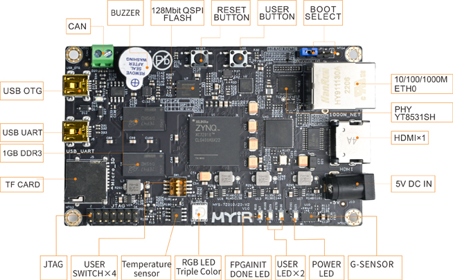
Some are accessed through Zynq’s PS part, while others through its PL.
Contents
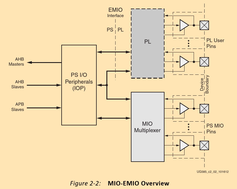
Block design

HDMI
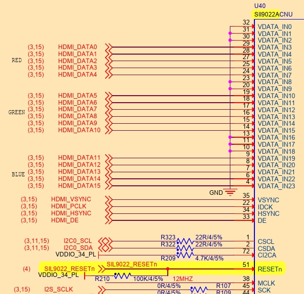
In order to find, where the HDMI is connected to, we can reference the schematics.
According to these, they are connected to the PL part (since PS pins would be numbered like MIO_#).
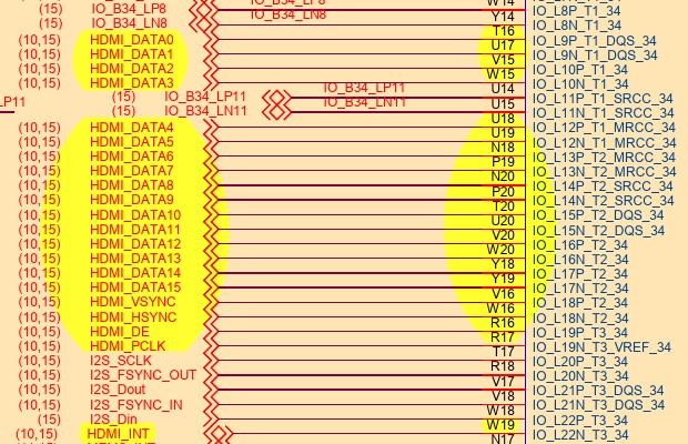
Looking further down [the schematics], we see that the signals pass through an “HDMI transmitter”.
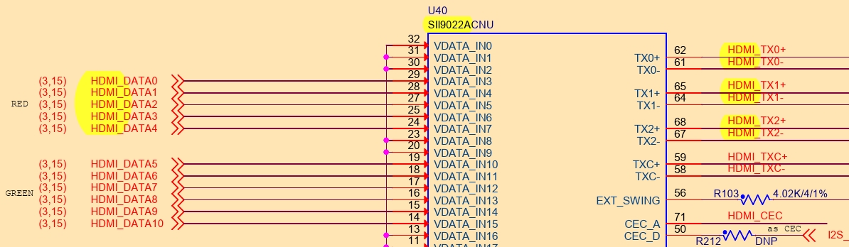
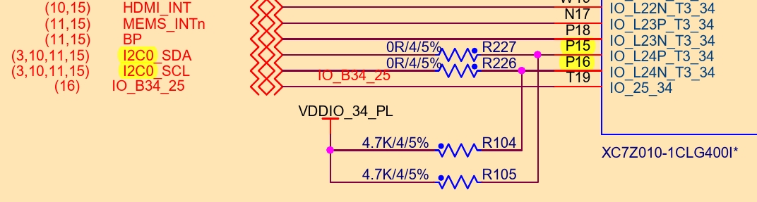
As a result, we have to power up the transmitter. In order to do so, we see that it communicates through the I2C-0 bus, thus we’ll need an I2C interface to do so.
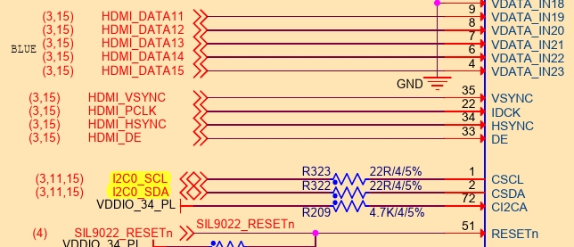
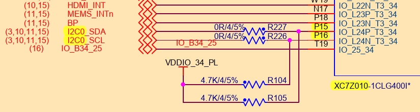
I2C-0 is connected to PL as P15 & P16
Activating Sil9022A
The minimal configuration needed is the following:
- Raise the
RESETnsignal [to power up Sil9022A] - Write
0x00to register0xC7, in order to enable the TPI (Transmitter Programming Interface) - Wait for ID to stabilize (at
0x1B-1D, 30). - Enable source termination (might be unnecessary, depending on the schematic/ external resistors)
- Disable TMDS output (at
0x1A) (default) - Switch from D2 to D0 state (at
0x1E) - Enable TMDS output (at
0x1A)
I2C Address
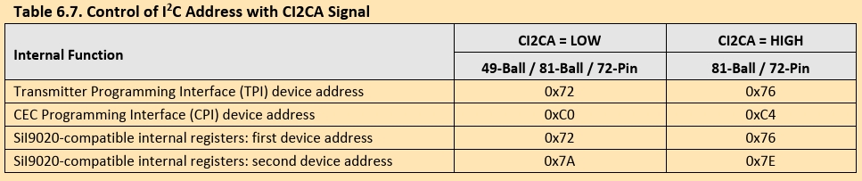
It’s important to note that the address is 0x3B. This derives from 0x76 » 1, which means that the datasheet depicts the 8-bit versions.
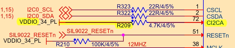
Needless to say, CI2CA has been raised (assuming R209 is in place).
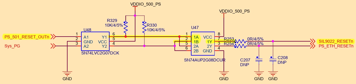
Raising RESETn
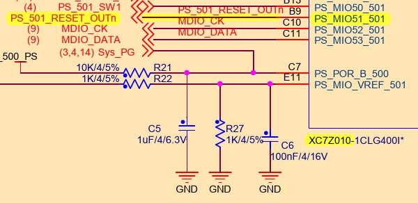
Searching through the schematics for the RESETn pin, we can see it’s connected to MIO51. (The signal passes first through a buffer and then through an AND gate).
Temperature sensor
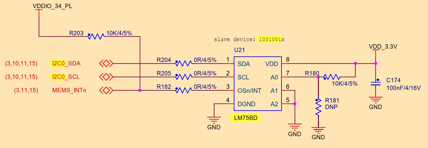
The temperature sensor, on board, is LM75B (NXP):
It’s an 11-bit ADC (with increments of 0.125°C)
The 7-bit [I2C] address is 0x49.
It is connected to I2C0, which is connected to PL pins P15 & P16. The provided contraints file has been set up.
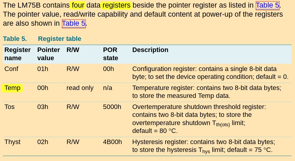
The sensor’s [temperature] register, is at address 00h. (It is 2 bytes long).
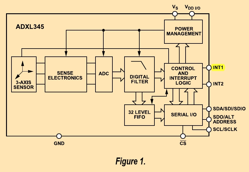
G-Sensor (acceleration sensor)
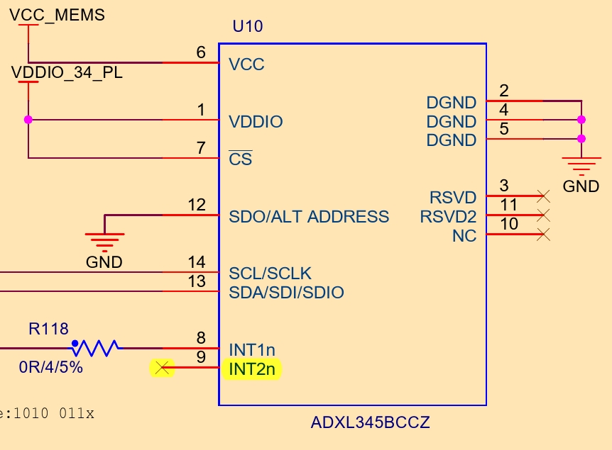
Referencing the schematics, the g-sensor, onboard, is the adlx345 from Analog Devices (datasheet).
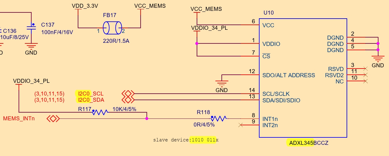
With 7-bit address 53h, over I2C0.
It has 3 axis of 13 bits, which give a resolution of 3.9 mg/LSB.
- Q: Can it detect variations in earth’s gravity?
- A: No. Maximum variation is around
0.069m/s²(0.7% ⋅ g) while we measure at0.035m/s²(0.36% ⋅ g) (1/282 ⋅ g).
I2C mode (disabled SPI)
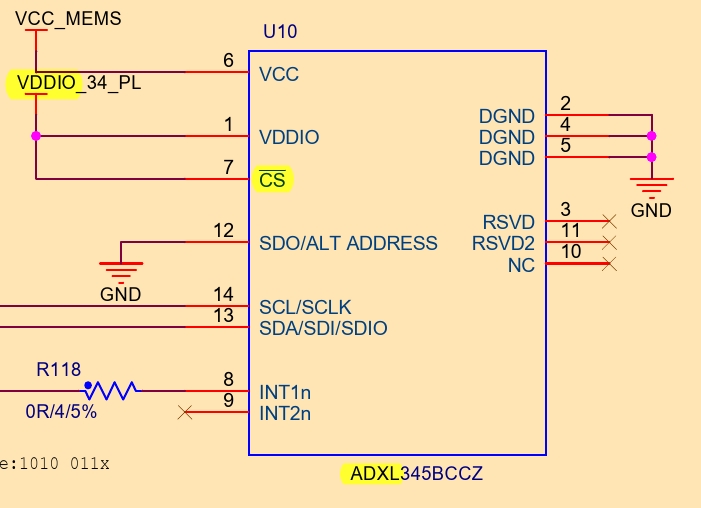
I2C communication mode is forced, due to C̅S̅ being tied to VDDIO (high).
Resolution
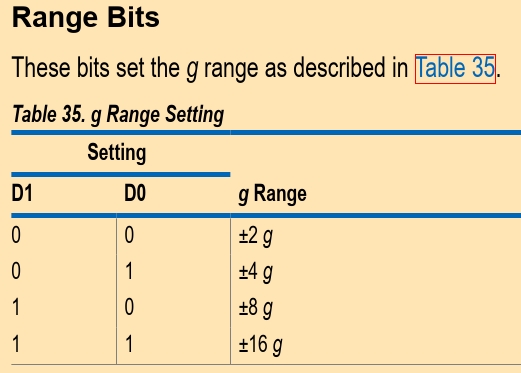
Maximum resolution can be achieved only when measuring around ±2 g.
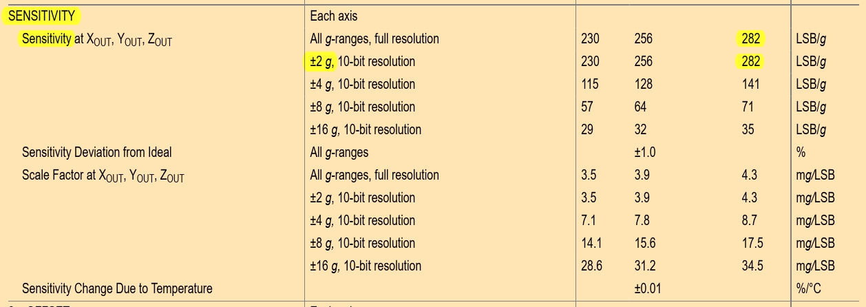
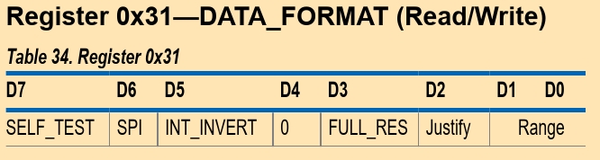
Settings are through the 0x31 register (named “DATA_FORMAT”), but they default to full resolution.
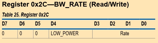
Sampling rate
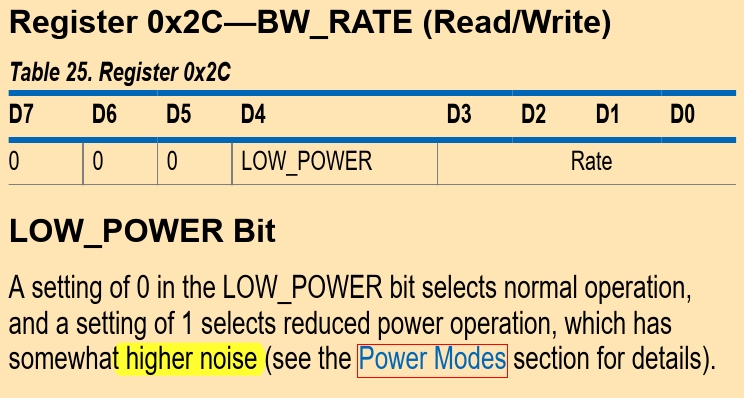
With a default sampling rate of 50Hz, maximum sampling rate can be achieved by setting the 0x2C register to 0x0F (which translates to 1600 Hz, due to there being 2 bytes per axis).
Spectral Analysis
DECLINED:
Doing an FFT only on the 32 samples (at maximum sampling rate) of the FIFO, would provide only 16 bins, which is too low a resolution, especially on the
1600Hzspan.
FUTURE:
Spectral analysis of nonuniformly sampled data can be achieved. This would be ideal, since it would span (?) the full spectrum of
1600Hz. Details in the docs/GDFT folder.
Wikipedia: Non-uniform discrete Fourier transform
Wikipedia: Least-squares spectral analysis ★★
Matlab: Spectral Analysis of Nonuniformly Sampled Signals
ACCEPTED:
Spectral analysis relative to I/O speed. That is, for a
100kHzI2C speed a50Hzsampling rate is allowed (half the data rate).
A low data rate of 100Hz should be preferred, against higher ones, due to the latter ones introducing noise.
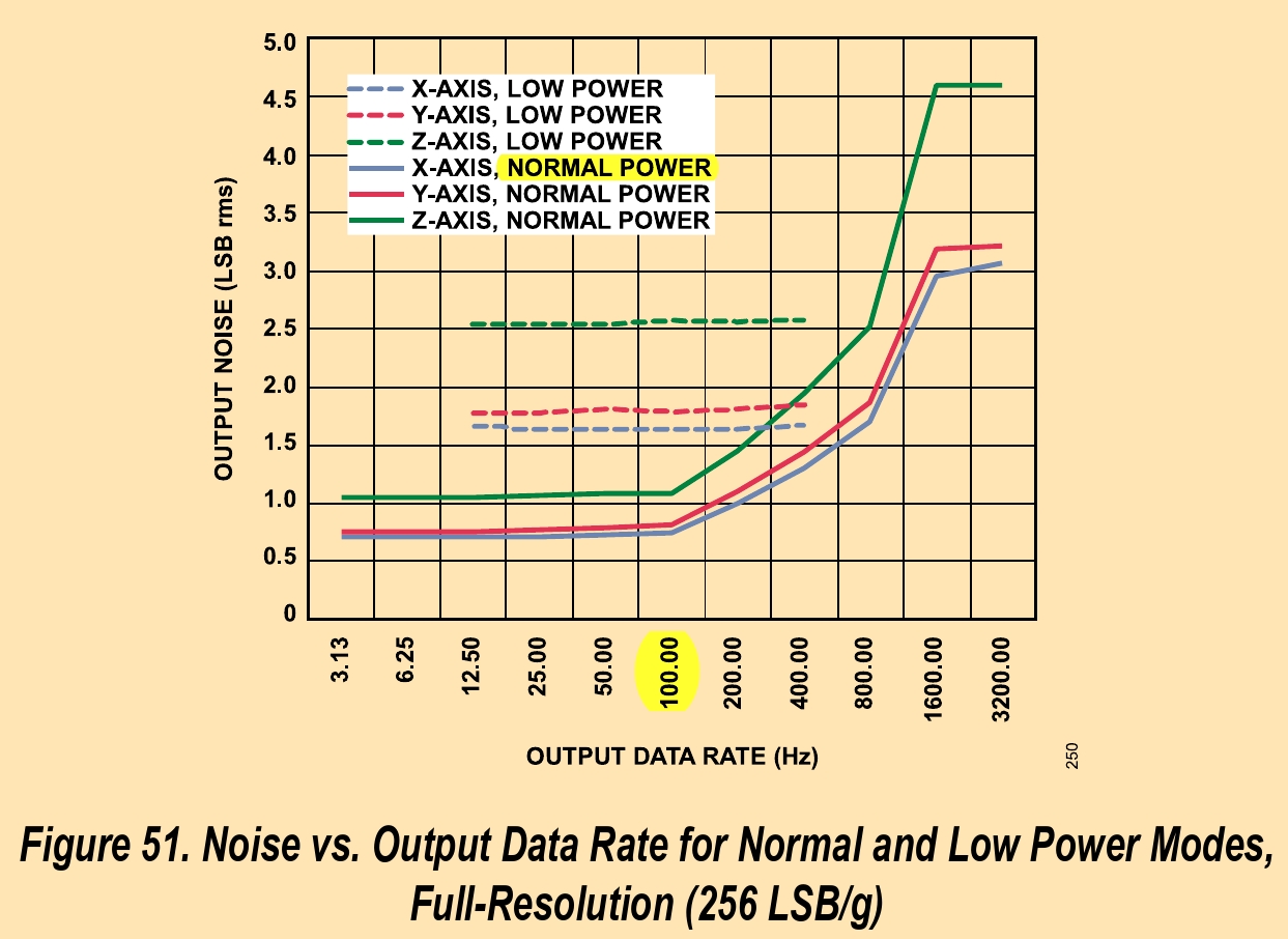
[Some] Lower (than 100Hz) data rates should also be avoided, since they introduce an offset, relative to temperature.
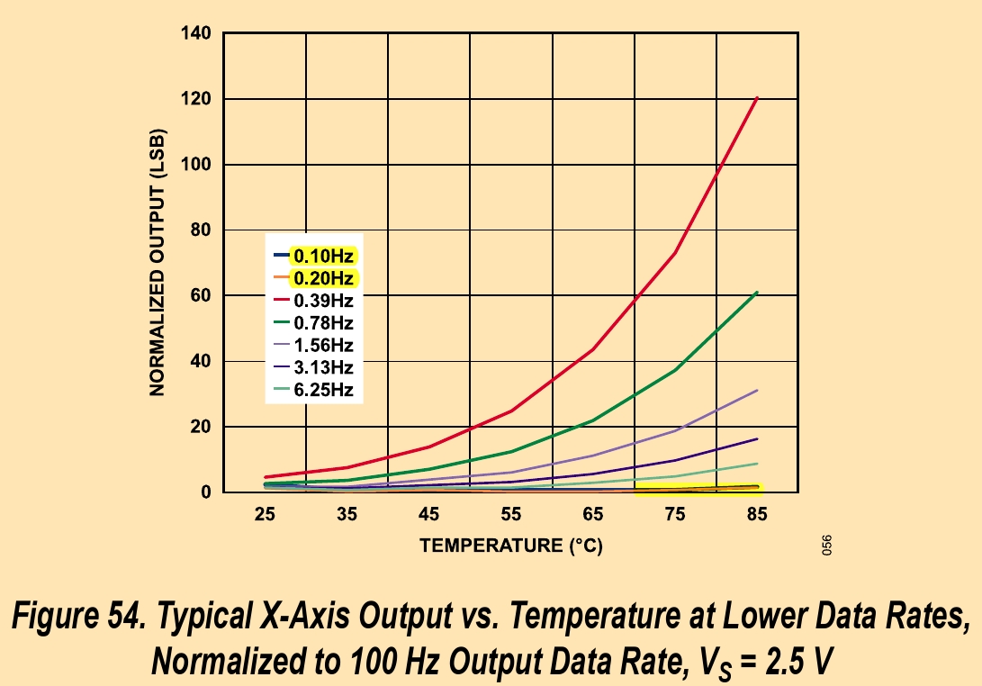
Low power [operation] should also be avoided as it introduces additional noise.
Data
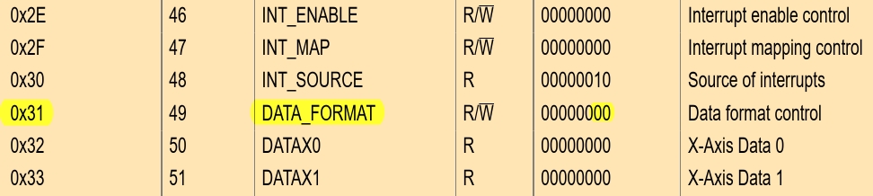
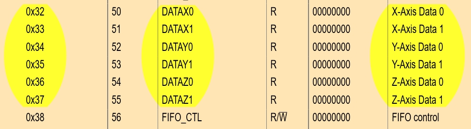
Data is stored as 3 sets of 2 bytes, at registers 0x32 to 0x37. They should be read as a 6-byte burst, to retain concurrency.
Trigger
For a consistent 100Hz sampling rate, we cannot use an external Timer as a trigger because the 2 interrupt pins are both output.
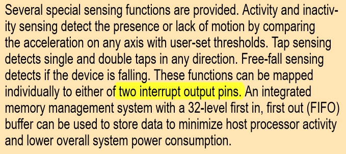
The 2nd interrupt pin is not connected.
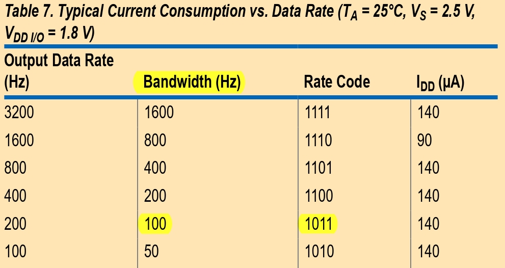
Thus, we shall program the ADXL to 100Hz, by setting the 0x2C register’s “Rate” field to 0b1011.
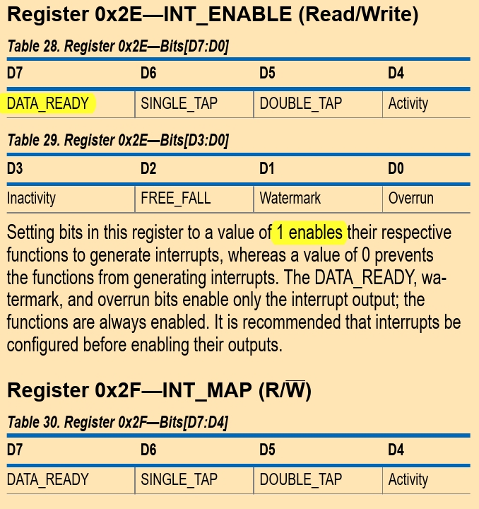
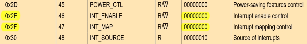
In order to signal DATA_READY on INT1 pin, we need to enable the “DATA_READY” field on 0x2E and keep it cleared on 0x2F.
The default values are the following.
Conclusion
- Interrupts to the PS, in order to maintain a target sampling rate
- Initial sampling rate of 50Hz (prototype). Final sampling rate of 1600Hz (difficulty when signal processing due to nonuniformly sampled data)
GPIO
The library being used is called Gpio-PS. API.
(All code has been provided). The general procedure is the following.
Gpio is first initialized:
- XGpioPs_LookupConfig() ▶ Retrieves the addresses assigned to the Gpio-PS controller and the related (parent?) interrupts
- XGpioPs_CfgInitialize() ▶ Sets the XGpioPs instance’s variables.
Next the pins are set:
- XGpioPs_SetDirectionPin() ▶ Which sets the pin as input/output
- XGpioPs_SetOutputEnablePin()
And written:
- XGpioPs_WritePin()
I2C
The library that’ll be used is the I2C-PS, with the respective API.
(All code has been provided). The general procedure is the following.
Initialization:
- XIicPs_LookupConfig(XIICPS_BASEADDRESS);
- XIicPs_CfgInitialize(&Iic, ConfigPtr, ConfigPtr->BaseAddress);
- XIicPs_SelfTest(&Iic);
- XIicPs_SetSClk(&Iic, IIC_SCLK_RATE);
Reading:
- XIicPs_BusIsBusy(&Iic)
- XIicPs_MasterSendPolled(&Iic, const_cast<uint8_t*>(v.data()), v.size(), SLAVE_ADDRESS); – Send register address, or an array of bytes (for Page/Offset referencies).
- XIicPs_BusIsBusy(&Iic)
- XIicPs_MasterRecvPolled(&Iic, result.data(), result.capacity(), SLAVE_ADDRESS); – Read register’s values